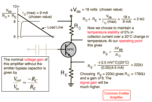
Common Emitter Amplifier Gain
共射极放大器增益
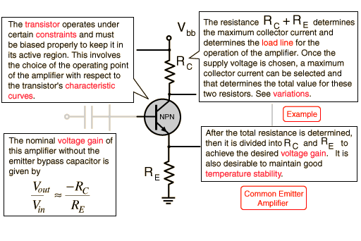
The collector voltage VC should be about half the supply voltage Vbbwhen there is no signal applied. This operating point allows a maximum swing of output voltage without clipping or distortion. One approach to design is to choose an operating collector current IC and then calculate the necessary collector resistor to drop from Vbb to that point. Choosing REwould then fix the load line and the gain.
当没有信号输入时,集电极电压V_C应约为电源电压V_bb的一半。这种工作点允许输出电压在不发生削波或失真的情况下达到最大摆幅。一种设计方法是选择一个工作集电极电流I_C,然后计算出所需的集电极电阻以从V_bb降至该点。选择R_E将确定负载线和增益。
Electronics concepts
索引电子学概念
| HyperPhysics*****Electricity and magnetism
HyperPhysics ***** 电磁学 | R Nave |
返回