Bilingual edition: English is preserved and Chinese follows each unit. Terminology uses the confirmed v20260916 glossary; automated semantic review remains traceable.
中英双语版:英文原文完整保留,中文紧随对应单元;术语采用 v20260916 确认表,自动语义审校结果可追溯。

Zener Regulator Design

齐纳稳压器设计

One approach to Zener regulator design is to consider the desired load current and the amount of ripple present in the available unregulated supply.
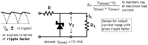
If the available power supply has
如果可用的功率供应有
= v ,
or ripple factor = %
或波纹系数 = %
中文译文中的待填/计算数值依次对应:1:rf。实际数值以上方原输入框为准。
and a zener voltage
以及一个泽纳电压
= V
Then to design for regulated output current of 0 to
然后设计为输出电流调节范围为0到
= mA
requires a resistor value
需要电阻值
=
This design with a load resistance
这种带有负载电阻的设计
=
will give an output current
将产生输出电流
= mA

Caution!! If this current is greater than the maximum design current you chose above, then it will not happen! You have chosen too small a load resistance. Also, the power values below will not be correct, because you are beyond the design range and will not be supplying enough voltage to the zener diode to allow it to give the zener voltage out.

注意!!如果这个电流大于你上面选择的最大设计电流,那么它就不会发生!你选择的负载电阻太小了。此外,下面的功率值也将不正确,因为你已经超出了设计范围,无法为齐纳二极管提供足够的电压以使其输出齐纳电压。
and output power
和输出功率
= W
To do this, it will require input power
这将需要输入功率
= W.

With this design approach, you must check the power ratings of your output resistor and Zener diode to make sure they are able to handle the power requirements.

采用这种设计方法时,必须检查输出电阻器和齐纳二极管的功率额定值,以确保它们能够满足功率需求。

The power rating of the load resistor must be at least
= W
and the power rating of the zener diode must be
= W

负载电阻的功率额定值必须至少为,并且齐纳二极管的功率额定值也必须为
中文译文中的待填/计算数值依次对应:1:pl 2:pz。实际数值以上方原输入框为准。

This design strategy is a practical, operational one: to design for a ripple-free output voltage up to a specified current maximum. Once done, you can choose load resistances which push the current up to this maximum and maintain regulation. However, it is easy to choose load resistances which push the current over the design maximum, and then the powers which this routine calculates will not be correct - they assume that the zener diode is operating at it's design voltage, and if you choose too small a load resistance, you drop the supply voltage at the zener below that voltage. The zener would then be acting like a voltage source, which of course it cannot do - it must have a supply voltage greater than the design voltage in order to regulate to that voltage.

这种设计策略是一种实用且可操作的策略:设计出在指定最大电流下无纹波的输出电压。一旦完成,你可以选择负载电阻,使电流达到这个最大值并保持调节。然而,很容易选择负载电阻使电流超过设计最大值,此时此程序计算的功率将不正确——它们假设齐纳二极管在其设计电压下工作,如果你选择过小的负载电阻,就会使齐纳二极管的供电电压低于该电压。此时齐纳二极管将像电压源一样工作,而实际上它不可能做到这一点——它必须有大于设计电压的供电电压才能实现调节。

Calculation note: You may substitute values for the zener voltage, the input voltage, the ripple voltage or ripple factor, and the load resistor. The other parameters will be calculated. Default values will be entered for unspecified parameters used in the calculation.

计算说明:您可以替换整流二极管的击穿电压、输入电压、纹波电压或纹波系数以及负载电阻的值。其他参数将被计算。在计算中未指定的参数将使用默认值。

Caution about use of the ripple factor: the relationship between the ripple factor and the amplitude of the ripple factor uses some details about the nature of common filters, and the numerical value of the ripple factor will be accurate only for rectified 60 Hz inputs where the ripple is fairly small. See the development of the ripple expression.

关于 ripple 因数的使用需注意:ripple 因数与 ripple 因数幅度之间的关系涉及一些关于常见滤波器特性的细节,只有在整流 60 Hz 输入且 ripple 较小时,ripple 因数的数值才准确。请参见 ripple 表达式的发展。
.
Alternate Design Strategy
替代设计策略
设计Zener调节器的一种方法是考虑所需的负载电流以及可用未调节电源中存在的纹波量。
中文译文中的待填/计算数值依次对应:1:vin 2:vrip 3:vz 4:r 5:rl 6:il 7:po 8:pin。实际数值以上方原输入框为准。
Index

Electronics concepts

Diode varieties
索引 电子学概念 二极管类型
 
HyperPhysics*****Electricity and magnetism
HyperPhysics ***** 电磁学
R Nave
Go Back
返回


计算模块中未附着于文字的输入框:
中文译文中的待填/计算数值依次对应:1:imax。实际数值以上方原输入框为准。