Silicon Crystal Structure
硅晶体结构
后Kittel |
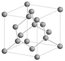
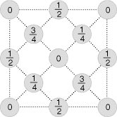 The above illustration shows the arrangement of the silicon atoms in a unit cell, with the numbers indicating the height of the atom above the base of the cube as a fraction of the cell dimension. 上述示意图显示了硅原子在单位胞中的排列情况,其中数字表示原子相对于立方体底面的高度,以单位胞尺寸的分数形式表示。 |
Silicon crystallizes in the same pattern as diamond, in a structure which Ashcroft and Mermin call "two interpenetrating face-centered cubic" primitive lattices. The lines between silicon atoms in the lattice illustration indicate nearest-neighbor bonds. The cube side for silicon is 0.543 nm. Germanium has the same diamond structure with a cell dimension of .566 nm.
硅晶体以与金刚石相同的方式结晶,其结构被称为“Ashcroft和Mermin所说的'两个相互穿插的面心立方'原始晶格”。晶格示意图中原子之间的线表示最近邻键。硅的立方边长为0.543 nm。锗具有相同的金刚石结构,其晶格常数为0.566 nm。
Semiconductor concepts
References
Kittel
Ashcroft & Mermin
半导体概念索引 参考文献 Kittel Ashcroft & Mermin
| HyperPhysics***** Condensed Matter
HyperPhysics ***** 凝聚态物理 | R Nave |
返回