Bilingual edition: English is preserved and Chinese follows each unit. Terminology uses the confirmed v20260916 glossary; automated semantic review remains traceable.
中英双语版:英文原文完整保留,中文紧随对应单元;术语采用 v20260916 确认表,自动语义审校结果可追溯。

The Junction Transistor

结型晶体管
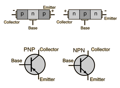
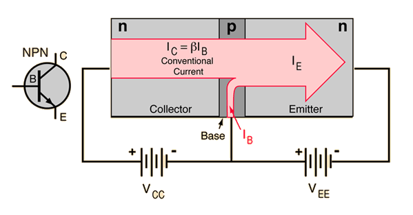
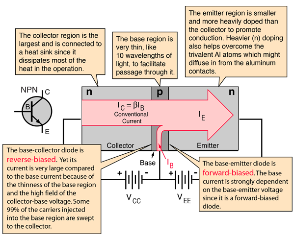
A bipolar junction transistor consists of three regions of doped semiconductors. A small current in the center or base region can be used to control a larger current flowing between the end regions (emitter and collector). The device can be characterized as a current amplifier, having many applications for amplification and switching.
双极型晶体管由三个掺杂半导体区域组成。中心或基区的微小电流可用于控制流经两端区域(发射极和集电极)的较大电流。该器件可被描述为电流放大器,具有广泛的应用于放大和开关的用途。
Constraints on operation
操作限制
Transistor operating conditions
晶体管的工作条件
Varieties of Transistors
晶体管的种类
Details about conduction in transistors
关于晶体管中的导电性细节
Determining collector current
确定集电极电流
Details about base-emitter junction
基极-发射极结的详细信息
Index

Semiconductor concepts

Semiconductors for electronics

Electronics concepts
索引 半导体概念 半导体在电子学中的应用 电子学概念
 
HyperPhysics***** Condensed Matter
HyperPhysics ***** 凝聚态物理
R Nave
Go Back
返回


Transistor as Current Amplifier

晶体管作为电流放大器

The larger collector current IC is proportional to the base current IB according to the relationship IC =βIB , or more precisely it is proportional to the base-emitter voltage VBE . The smaller base current controls the larger collector current, achieving current amplification.

较大的集电极电流I_C与基极电流I_B成正比,关系为I_C = βI_B,更准确地说,它与基极-发射极电压V_BE成正比。较小的基极电流控制较大的集电极电流,实现电流放大。

The analogy to a valve is sometimes helpful. The smaller current in the base acts as a "valve", controlling the larger current from collector to emitter. A "signal" in the form of a variation in the base current is reproduced as a larger variation in the collector-to-emitter current, achieving an amplification of that signal.

将晶体管类比为阀门有时很有帮助。基极中的较小电流起到‘阀门’的作用,控制从集电极到发射极的较大电流。以基极电流的变化形式传递的‘信号’,会以更大的集电极到发射极电流变化形式再现,从而实现对信号的放大。
Constraints on operation
操作限制
Comments on structure
关于结构的评论
To pnp version
转为PNP版本
Index

Semiconductor concepts

Semiconductors for electronics

Electronics concepts

Reference
Diefenderfer /Holton
p156
索引 半导体概念 半导体在电子学中的应用 电子学概念 参考 Diefenderfer /Holton p156
 
HyperPhysics***** Condensed Matter
HyperPhysics ***** 凝聚态物理
R Nave
Go Back
返回


Transistor Structure

晶体管结构

The junction transistor
结型晶体管
Current amplifier operation
电流放大操作
Constraints on operation
操作限制
Index

Semiconductor concepts

Semiconductors for electronics

Electronics concepts
索引 半导体概念 半导体在电子学中的应用 电子学概念
 
HyperPhysics***** Condensed Matter
HyperPhysics ***** 凝聚态物理
R Nave
Go Back
返回


Transistor as Current Amplifier

晶体管作为电流放大器

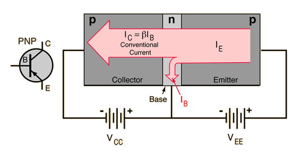
The larger collector current IC is proportional to the base current IB according to the relationship IC =βIB , or more precisely it is proportional to the base-emitter voltage VBE . The smaller base current controls the larger collector current, achieving current amplification.

较大的集电极电流I_C与基极电流I_B成正比,关系为I_C = βI_B,更准确地说,它与基极-发射极电压V_BE成正比。较小的基极电流控制较大的集电极电流,实现电流放大。
Constraints on operation
操作限制
To npn version
npn 版本
Index

Semiconductor concepts

Semiconductors for electronics

Electronics concepts
索引 半导体概念 半导体在电子学中的应用 电子学概念
 
HyperPhysics***** Condensed Matter
HyperPhysics ***** 凝聚态物理
R Nave
Go Back
返回


Constraints on Transistor Operation

晶体管操作的限制
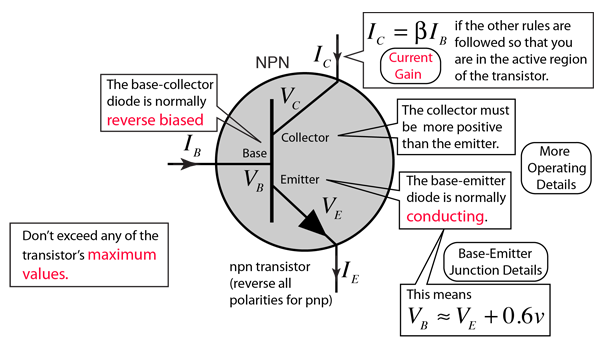
The bold text and the "buttons" are active links to further details.
粗体文本和‘按钮’是指向更多细节的活动链接。
Index

Semiconductor concepts

Semiconductors for electronics

Electronics concepts
索引 半导体概念 半导体在电子学中的应用 电子学概念
 
HyperPhysics***** Condensed Matter
HyperPhysics ***** 凝聚态物理
R Nave
Go Back
返回


Transistor Maximum Values

晶体管最大值

Part of the manufacturer's data for transistors is a set of maximum values which must not be exceeded in its operation. These form some of the constraints on transistor operation which are a part of the design of any circuit. A typical set, for the silicon transistor 2N2222:

晶体管制造商的数据中的一部分是一组最大值,其在操作中不得超过。这些构成了晶体管操作的一些约束,是任何电路设计的一部分。对于硅晶体管2N2222,一个典型的数据集为:
  • Collector-Base Voltage = 60 v
    集电极-基极电压 = 60 v
  • Collector-Emitter Voltage = 30 v
    集电极-发射极电压 = 30 v
  • Base-Emitter Voltage = 5 v
    基-射极电压 = 5 v
  • Power dissipation = 500 mW
    功率耗散 = 500 mW
  • Temperature 125 C
    温度 125 摄氏度
Index

Semiconductor concepts

Semiconductors for electronics

Electronics concepts
索引 半导体概念 半导体在电子学中的应用 电子学概念
 
HyperPhysics***** Condensed Matter
HyperPhysics ***** 凝聚态物理
R Nave
Go Back
返回