Bilingual edition: English is preserved and Chinese follows each unit. Terminology uses the confirmed v20260916 glossary; automated semantic review remains traceable.
中英双语版:英文原文完整保留,中文紧随对应单元;术语采用 v20260916 确认表,自动语义审校结果可追溯。

Transistor Operation

晶体管操作
A transistor in a circuit will be in one of three conditions
  1. Cut off (no collector current), useful for switch operation.
    截止(无集电极电流),适用于开关操作
  2. In the active region (some collector current, more than a few tenths of a volt above the emitter), useful for amplifier applications
    在放大区(某些集电极电流, emitter 电压高于几 tenths 伏), 适用于放大器应用
  3. In saturation (collector a few tenths of a volt above emitter), large current useful for "switch on" applications.
    在饱和区(集电极略高于发射极几十分之一伏),有较大的电流,适用于'导通'应用。
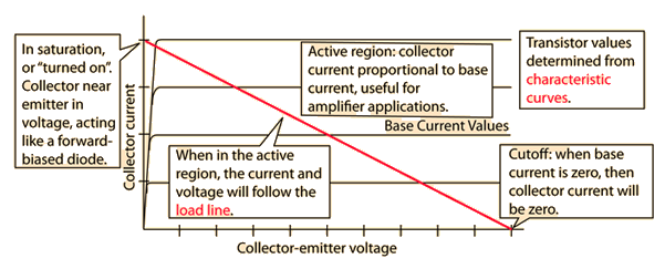
Transistor load line
晶体管负载线
Characteristic curves
特征曲线
电路中的晶体管将处于三种状态中的一种
Index

Semiconductor concepts

Semiconductors for electronics
索引 半导体概念 半导体在电子学中的应用
 
HyperPhysics***** Condensed Matter
HyperPhysics ***** 凝聚态物理
R Nave
Go Back
返回


Collector Current Determination

集电极电流确定

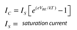
The base-emitter voltage VBE can be considered to be the controlling variable in determining transistor action. The collector current is related to this voltage by the Ebers-Moll relationship (sometimes labeled the Shockley equation):

where
其中
The saturation current is characteristic of the particular transistor (a parameter which itself has a temperature dependence). This relationship is stable over a wide range of voltages and currents. A further useful relationship is
IC=βIB where β can be called the current gain. The value of β is not highly dependable since it depends on IC , VCE, and the temperature.
其中β可以称为电流增益。由于β取决于I_C、V_CE和温度,其值并不十分可靠。
基极-发射极电压V_BE可以被视为确定晶体管作用的控制变量。集电极电流与该电压之间的关系由埃伯斯-莫尔关系(有时称为肖克利方程)描述:饱和电流是特定晶体管的特性(一个本身具有温度依赖性的参数)。这种关系在广泛的电压和电流范围内都保持稳定。另一个有用的 relationship 是
Index

Semiconductor concepts

Semiconductors for electronics

References
Horowitz & Hill
Sec. 2.10

Floyd
Electronic Devices, Appendix B
索引 半导体概念 半导体在电子学中的应用 参考文献 Horowitz & Hill 第2.10节 Floyd 电子器件,附录B
 
HyperPhysics***** Condensed Matter
HyperPhysics ***** 凝聚态物理
R Nave
Go Back
返回


Base-Emitter Junction Details

基极-发射极接点细节
Some useful "rules of thumb" which help in understanding transistor action are (from Horowitz & Hill):
  1. A base emitter voltage VBE of about 0.6 v will "turn on" the base-emitter diode and that voltage changes very little, < +/- 0.1v throughout the active range of the transistor which may change base current by a factor of 10 or more.
    当基极-发射极二极管的发射极电压V_BE约为0.6 V时,该二极管会被“导通”,且在此晶体管的活动范围内,该电压变化非常小,小于±0.1 V,这种变化可能使基极电流增加10倍或更多。
  2. An increase in base-emitter voltage VBE by about 60 mV will increase the collector current IC by about a factor of 10.
  3. The effective AC series resistance of the emitter is about 25/IC ohms.
    发射极的有效交流串联电阻约为25/I_C欧姆。
  4. The base-emitter voltage VBE is temperature dependent, decreasing about 2.1 mV/C
    基-射极电压V_BE具有温度依赖性,约每下降2.1 mV/C
  5. The base-emitter voltage VBE varies slightly with the collector-emitter voltage VCE at constant collector current IC : ΔVBE ≈ -0.001ΔVCE.
    基-射极电压V_BE在集电极电流I_C恒定时,随着集电极-射极电压V_CE略有变化:ΔV_BE ≈ -0.001ΔV_CE。
  6. 基极-发射极电压V_BE增加约60 mV时,集电极电流I_C将增加约10倍。
Base-emitter Voltage Curve
基极-发射极电压曲线
一些有助于理解晶体管作用的‘粗略规则’(来自Horowitz & Hill):
Index

Reference
Horowitz & Hill
Sec 2.10

Semiconductor concepts

Semiconductors for electronics
索引参考Horowitz & Hill第2.10节半导体概念半导体用于电子学
 
HyperPhysics***** Condensed Matter
HyperPhysics ***** 凝聚态物理
R Nave
Go Back
返回


Transistor Action

晶体管作用
More on transistor regions
关于晶体管区域的更多内容
Index

Semiconductor concepts

Semiconductors for electronics

Reference
Simpson
Ch 5
索引 半导体概念 半导体在电子学中的应用 参考 Simpson 第5章
 
HyperPhysics***** Condensed Matter
HyperPhysics ***** 凝聚态物理
R Nave
Go Back
返回


More about transistor regions

关于晶体管区域的更多内容
Transistor action
晶体管作用
Index

Semiconductor concepts

Semiconductors for electronics
索引 半导体概念 半导体在电子学中的应用
 
HyperPhysics***** Condensed Matter
HyperPhysics ***** 凝聚态物理
R Nave
Go Back
返回


Collector Current

集电极电流

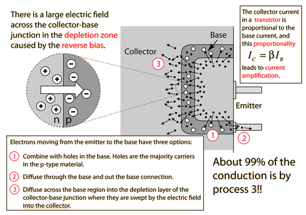
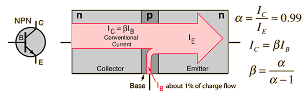
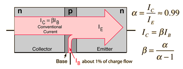
Normal transistor action results in a collector-to-emitter current which is about 99% of the total current. The usual symbols used to express the transistor current relationships are shown.

正常晶体管工作时,集电极到发射极的电流约为总电流的99%。用来表示晶体管电流关系的常用符号如图所示。

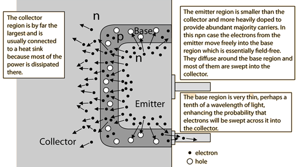
The proportionality β can take values in the range 20 to 200 and is not a constant even for a given transistor. It increases for larger emitter currents because the larger number of electrons injected into the base exceeds the available holes for recombination so the fraction which recombine to produce base current delines even further.

比例系数β的取值范围在20到200之间,并且即使对于同一晶体管来说,它也不是一个常数。随着发射极电流增大,β会增加,因为注入基区的电子数量增多,超过可重组的空穴数量,因此参与产生基极电流的重组分数进一步减少。
Use of the current gain beta.
电流增益β的使用
Index

Semiconductor concepts

Semiconductors for electronics
索引 半导体概念 半导体在电子学中的应用
 
HyperPhysics***** Condensed Matter
HyperPhysics ***** 凝聚态物理
R Nave
Go Back
返回


Use of the Current Gain

电流增益的使用

Any circuit that depends on a specific value of the current gain β is a bad circuit because that value varies for a given transistor as well as between different transistors of the same type.

The current gain is useful for:
Design of the biasing circuits
偏置电路的设计
Common Emitter
共射极
Common Collector
共集电极
Calculation of impedances
阻抗的计算
Common Emitter
共射极
Common Collector
共集电极
任何依赖特定β值的电路都是一个坏电路,因为对于给定的晶体管,该值会变化,而且相同类型的不同晶体管之间也会有差异。电流增益在以下方面是有用的:
Index

Semiconductor concepts

Semiconductors for electronics
索引 半导体概念 半导体在电子学中的应用
 
HyperPhysics***** Condensed Matter
HyperPhysics ***** 凝聚态物理
R Nave
Go Back
返回