Junction Field Effect Transistor
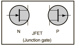 |
The common transistor is called a junction transistor, and it was the key device which led to the solid state electronics revolution. In application, the junction transistor has the disadvantage of a low input impedance because the base of the transistor is the signal input and the base-emitter diode is forward biased. Another device achieved transistor action with the input diode junction reversed biased, and this device is called a "field effect transistor" or a "junction field effect transistor", JFET. With the reverse biased input junction, it has a very high input impedance. Having a high input impedance minimizes the interference with or "loading" of the signal source when a measurement is made. 常见的晶体管称为结型晶体管,它是导致固体电子学革命的关键器件。在应用中,结型晶体管的缺点是输入阻抗较低,因为晶体管的基极是信号输入,而基极-发射极二极管处于正向偏置状态。另一种器件通过将输入二极管 junction 反向偏置实现了晶体管作用,这种器件称为“场效应晶体管”或“结型场效应晶体管”,即JFET。由于输入 junction 反向偏置,它具有非常高的输入阻抗。高输入阻抗可以最小化对信号源的干扰或“负载效应”,从而在测量时减少干扰。
|
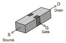 |
For an n-channel FET, the device is constructed from a bar of n-type material, with the shaded areas composed of a p-type material as a Gate. Between the Source and the Drain, the n-type material acts as a resistor. The current flow consists of the majority carriers (electrons for n-type material). 对于n沟道FET,器件由一块n型材料制成,其中阴影区域由p型材料构成作为门极。在源极和漏极之间,n型材料起着电阻的作用。电流流动由多数载流子(对于n型材料而言是电子)组成。
|
Since the Gate junction is reverse biased and because there is no minority carrier contribution to the flow through the device, the input impedance is extremely high.
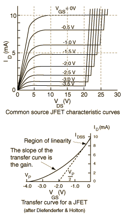
The control element for the JFET comes from depletion of charge carriers from the n-channel. When the Gate is made more negative, it depletes the majority carriers from a larger depletion zone around the gate. This reduces the current flow for a given value of Source-to-Drain voltage. Modulating the Gate voltage modulates the current flow through the device.
Electronics concepts
Transistor varieties
Reference
Diefenderfer & Holton
Sec 8-7
| HyperPhysics*****Electricity and magnetism
HyperPhysics ***** 电磁学 | R Nave |