Bilingual edition: English is preserved and Chinese follows each unit. Terminology uses the confirmed v20260916 glossary; automated semantic review remains traceable.
中英双语版:英文原文完整保留,中文紧随对应单元;术语采用 v20260916 确认表,自动语义审校结果可追溯。

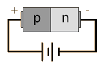
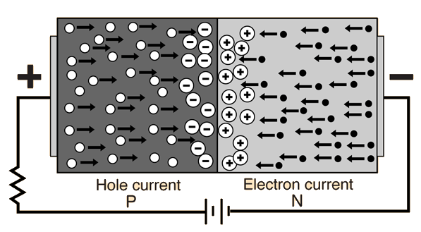
Forward Biased P-N Junction

正向偏置的P-N结

Forward biasing the p-n junction drives holes to the junction from the p-type material and electrons to the junction from the n-type material. At the junction the electrons and holes combine so that a continuous current can be maintained.
在p-n结上施加正向偏置时,空穴会从p型材料向结移动,电子会从n型材料向结移动。在结处,电子和空穴结合,从而可以维持持续的电流。
Show energy bands.
显示能带
Compare to reverse bias.
与反向偏置比较
Index

Semiconductor concepts

Semiconductors for electronics
索引 半导体概念 半导体在电子学中的应用
 
HyperPhysics***** Condensed Matter
HyperPhysics ***** 凝聚态物理
R Nave
Go Back
返回


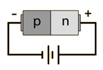
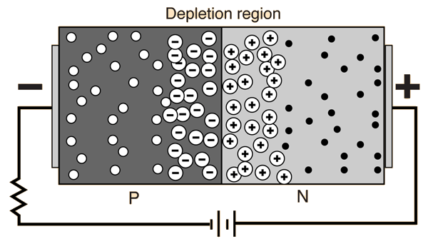
Reverse Biased P-N Junction

反向偏置的P-N结

The application of a reverse voltage to the p-n junction will cause a transient current to flow as both electrons and holes are pulled away from the junction. When the potential formed by the widened depletion layer equals the applied voltage, the current will cease except for the small thermal current.
当反向电压施加于p-n结时,电子和空穴会被拉离结区,从而产生一个瞬时电流。当由扩宽的耗尽层形成的电势等于施加电压时,电流将停止,仅留下微小的热电流。
Show energy bands.
显示能带
Compare to forward bias.
与正向偏置相比
Index

Semiconductor concepts

Semiconductors for electronics
索引 半导体概念 半导体在电子学中的应用
 
HyperPhysics***** Condensed Matter
HyperPhysics ***** 凝聚态物理
R Nave
Go Back
返回


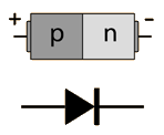
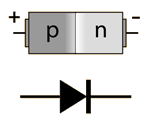
The P-N Junction Diode

P-N 接面二极体

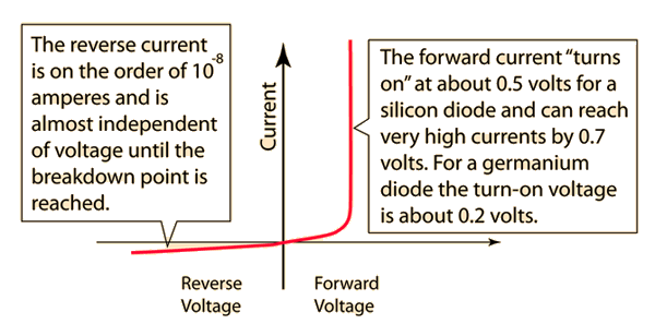
The nature of the p-n junction is that it will conduct current in the forward direction but not in the reverse direction. It is therefore a basic tool for rectification in the building of DC power supplies.
PN结的特性是它会在正向方向导通电流,而在反向方向不导通电流。因此,它是构建直流电源时实现整流的基本工具。
Diode varieties
二极管类型
PIN diode
PIN二极管
Step-recovery diode
阶梯恢复二极管
Diode applications
二极管应用
Index

Semiconductor concepts

Semiconductors for electronics
索引 半导体概念 半导体在电子学中的应用
 
HyperPhysics***** Condensed Matter
HyperPhysics ***** 凝聚态物理
R Nave
Go Back
返回


The PIN Diode

PIN二极管

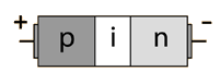
The PIN diode has heavily doped p-type and n-type regions separated by an intrinsic region. When reverse biased, it acts like an almost constant capacitance and when forward biased it behaves as a variable resistor.

PIN二极管有高度掺杂的p型和n型区域,由本征区隔开。当反向偏置时,它表现出几乎恒定的电容;当正向偏置时,它则表现为可变电阻。
The forward resistance of the intrinsic region decreases with increasing current. Since its forward resistance can be changed by varying the bias, it can be used as a modulating device for AC signals. It is used in microwave switching applications.
内在区域的正向电阻随电流增加而减小。由于可以通过改变偏置来改变其正向电阻,因此可以作为交流信号的调制器件。它用于微波开关应用。
Index

Semiconductor concepts

Semiconductors for electronics
索引 半导体概念 半导体在电子学中的应用
 
HyperPhysics***** Condensed Matter
HyperPhysics ***** 凝聚态物理
R Nave
Go Back
返回


Step-Recovery Diode

步降二极管

In the step-recovery diode the doping level is gradually decreased as the junction is approached. This reduces the switching time since the smaller amount of stored charge near the junction can be released more rapidly when changing from forward to reverse bias.

在阶梯恢复二极管中,随着接近结,掺杂浓度逐渐降低。这会减少开关时间,因为靠近结处的存储电荷较少,当从正向偏置切换到反向偏置时可以更快地释放。
The forward current can also be established more rapidly than in the ordinary junction diode. This diode is used in fast switching applications.
正向电流也可以比普通结型二极管更迅速地建立。这种二极管用于快速开关应用。
Index

Semiconductor concepts

Semiconductors for electronics
索引 半导体概念 半导体在电子学中的应用
 
HyperPhysics***** Condensed Matter
HyperPhysics ***** 凝聚态物理
R Nave
Go Back
返回