Light Detectors光探测器
|
Index Optoelectronics concepts Electronics concepts 索引光电概念电子概念 | ||||
|
Go Back
返回 |
Photoresistors光敏电阻
Low cost, two lead photoresistors using a cadmium sulfide (CdS) element show a dramatic decrease in resistance when illuminated and are commonly used as a light sensing element for security lights, etc. so that they will turn on at night. In the dark, the resistance is very high, in the 1 megohm range. When illuminated, the resistance may drop to a few hundred ohms. They are typically more sensitive to green light, and they have a very high sensitivity compared to other types of sensors. They cannot be practically used for high speed switching or modulation for communications purposes because there is a "memory effect", requiring on the order of a second for the resistance to rise to its dark resistance. 低成本的双引脚光敏电阻使用硫化镉(CdS)元件,当被光照时电阻会显著下降,常用于安全灯等的光感应元件,以便在夜间开启。在黑暗中,其电阻非常高,大约在1兆欧范围内。当被光照时,电阻可能降至几百欧姆。它们对绿色光更为敏感,其灵敏度相比其他类型的传感器非常高。由于存在“记忆效应”,它们无法实际用于高速开关或通信调制,因为电阻要上升到暗处电阻需要约1秒的时间。
![]() |
Index Electronics concepts Optoelectronics concepts 索引 电子学概念 光电子学概念 | ||
|
Go Back
返回 |
Solar Cells太阳能电池
Silicon photovoltaic cells are typically thought of as voltage supplies, but they are also useful as sensitive detectors of light and near infrared. Solar cells are silicon wafers which are doped to produce a p-n junction. Commonly used "cells" are produced as wafers of diameter about 8 cm and 3 mm thickness which are cut from a crystalline silicon rod. The thin wafer is doped on one side to produce p-material (e.g., boron doped silicon) and on the other side to produce n-material (e.g., phosphorous doped silicon). The p material is typically connected to a metal base and the top side of the wafer (n-type) has a grid of electrical contacts. When light strikes the top of the wafer, it can penetrate through the p-n junctions and free electrons which can cross the junction into the n-type region. Electrons are then held in the n-region, being unable to recross the junction into the p-region. This establishes a voltage of about 0.5 volts and a cell as described above can produce about 1 watt of electrical output. 硅光电池通常被视为电压源,但它们也能够作为对光和近红外线敏感的探测器。太阳能电池是经过掺杂以形成p-n结的硅薄片。常用的“电池”是直径约为8厘米、厚度3毫米的薄片,这些薄片是从单晶硅棒中切割出来的。薄片的一侧被掺杂以形成p区(例如,掺硼的硅),另一侧被掺杂以形成n区(例如,掺磷的硅)。p区通常连接到金属基座,而薄片的顶部(n型)则有网格状的电接触点。当光照射到薄片顶部时,它可以穿透p-n结和自由电子,这些电子可以跨越结进入n区。电子随后被限制在n区,无法再返回到p区。这建立了约0.5伏的电压,如上所述的电池可以产生约1瓦的电输出。
|
Index Electronics concepts Optoelectronics concepts References Mims, Forrest, Optoelectronic Circuits 索引 电子学概念 光电子学概念 参考文献 Mims, Forrest, 光电子电路 | ||
|
Go Back
返回 |
Phototransistors光敏晶体管
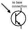
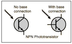
A standard transistor is a three-lead device, and although the phototransistor has three regions, typically NPN, the base region is enlarged and generally does not have a lead attached to it. The collector-base junction is sensitive to light falling on it; a base current proportional to the light intensity is produced. This initiates a collector current proportional to the light intensity. 标准晶体管是一种三端器件,尽管光晶体管有三个区域,通常为NPN型,但基区被扩大,通常不连接引线。集电极-基极结对落在其上的光敏感;会产生与光强度成正比的基极电流。这会引发与光强度成正比的集电极电流。
|
Index Electronics concepts Optoelectronics concepts 索引 电子学概念 光电子学概念 | ||
|
Go Back
返回 |
Phototransistor光敏晶体管
|
Index Electronics concepts Optoelectronics concepts 索引 电子学概念 光电子学概念 | ||
|
Go Back
返回 |