Bilingual edition: English is preserved and Chinese follows each unit. Terminology uses the confirmed v20260916 glossary; automated semantic review remains traceable.
中英双语版:英文原文完整保留,中文紧随对应单元;术语采用 v20260916 确认表,自动语义审校结果可追溯。

P-N Junction

P-N结

One of the crucial keys to solid state electronics is the nature of the P-N junction. When p-type and n-type materials are placed in contact with each other, the junction behaves very differently than either type of material alone. Specifically, current will flow readily in one direction (forward biased) but not in the other (reverse biased), creating the basic diode. This non-reversing behavior arises from the nature of the charge transport process in the two types of materials.
固体电子学中的一个关键问题是P-N结的性质。当P型和N型材料接触时,结的行为与单独的材料类型完全不同。具体来说,电流在一个方向(正向偏置)中容易流动,而在另一个方向(反向偏置)中则不流动,从而形成基本的二极管。这种不可逆的行为源于两种材料中电荷输运过程的性质。

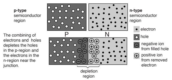
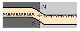
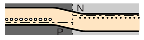
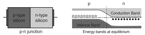
The open circles on the left side of the junction above represent "holes" or deficiencies of electrons in the lattice which can act like positive charge carriers. The solid circles on the right of the junction represent the available electrons from the n-type dopant. Near the junction, electrons diffuse across to combine with holes, creating a "depletion region". The energy level sketch above right is a way to visualize the equilibrium condition of the P-N junction. The upward direction in the diagram represents increasing electron energy.

在结的左侧,开放的圆圈代表“空穴”或晶格中电子的缺失,这些可以像正电荷载体一样起作用。结的右侧的实心圆圈代表来自n型掺杂的可用电子。在结附近,电子扩散到与空穴结合,形成一个“耗尽区”。上方右图的能级示意图是一种可视化P-N结平衡状态的方式。图中向上的方向表示电子能量的增加。
Electron and hole conduction
电子和空穴导电
Index

Semiconductor concepts

Semiconductors for electronics
索引 半导体概念 半导体在电子学中的应用
 
HyperPhysics***** Condensed Matter
HyperPhysics ***** 凝聚态物理
R Nave
Go Back
返回


Depletion Region

去除区

When a p-n junction is formed, some of the free electrons in the n-region diffuse across the junction and combine with holes to form negative ions. In so doing they leave behind positive ions at the donor impurity sites.

当形成p-n结时,一些自由电子从n区扩散到结的另一侧,与空穴结合形成负离子。在此过程中,它们在施主杂质位点留下正离子。
Show more detail of depletion region.
depletion 区域的更多细节
Index

Semiconductor concepts

Semiconductors for electronics
索引 半导体概念 半导体在电子学中的应用
 
HyperPhysics***** Condensed Matter
HyperPhysics ***** 凝聚态物理
R Nave
Go Back
返回


Depletion Region Details

耗尽区详情
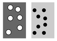
In the p-type region there are holes from the acceptor impurities and in the n-type region there are extra electrons.
在p型区域存在来自受主杂质的空穴,在n型区域存在额外的电子。
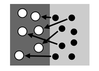
When a p-n junction is formed, some of the electrons from the n-region which have reached the conduction band are free to diffuse across the junction and combine with holes.
当形成p-n结时,一些从n区跃迁到导带的电子可以扩散过结并与空穴结合。
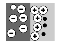
Filling a hole makes a negative ion and leaves behind a positive ion on the n-side. A space charge builds up, creating a depletion region which inhibits any further electron transfer unless it is helped by putting a forward bias on the junction.
填充电极孔会生成负离子,并在n侧留下正离子。由此形成空间电荷区,抑制了进一步的电子转移,除非施加正向偏置电压以帮助电子转移。
Show effects of biasing.
展示偏置效应。
Index

Semiconductor concepts

Semiconductors for electronics
索引 半导体概念 半导体在电子学中的应用
 
HyperPhysics***** Condensed Matter
HyperPhysics ***** 凝聚态物理
R Nave
Go Back
返回


Bias effect on electrons in depletion zone

偏置效应对耗尽区电子的影响
Equilibrium of junction

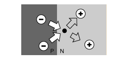
Coulomb force from ions prevents further migration across the p-n junction. The electrons which had migrated across from the N to the P region in the forming of the depletion layer have now reached equilibrium. Other electrons from the N region cannot migrate because they are repelled by the negative ions in the P region and attracted by the positive ions in the N region.

库仑力阻止了离子进一步迁移过p-n结。在形成耗尽层时,从N区迁移至P区的电子现在已经达到平衡。其他来自N区的电子无法迁移,因为它们被P区中的负离子排斥,又被N区中的正离子吸引。
节点平衡
Reverse bias

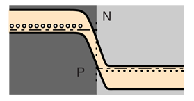
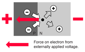
An applied voltage with the indicated polarity further impedes the flow of electrons across the junction. For conduction in the device, electrons from the N region must move to the junction and combine with holes in the P region. A reverse voltage drives the electrons away from the junction, preventing conduction.

施加的电压 polarity 进一步阻碍了电子跨结的流动。对于器件的导电,N 区的电子必须移动到结并结合 P 区的空穴。反向电压会将电子驱离结,阻止导电。
反向偏置
Forward bias

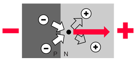
An applied voltage in the forward direction as indicated assists electrons in overcoming the coulomb barrier of the space charge in the depletion region. Electrons will flow with very small resistance in the forward direction.

在正向方向施加的电压如图所示,有助于电子克服 depletion 区内空间电荷的库仑势垒。电子在正向方向流动时具有非常小的电阻。
正向偏置
Click on one of the junction conditions for more detail.
点击了解其中一个接合条件的更多细节。
Index

Semiconductor concepts

Semiconductors for electronics
索引 半导体概念 半导体在电子学中的应用
 
HyperPhysics***** Condensed Matter
HyperPhysics ***** 凝聚态物理
R Nave
Go Back
返回