Bilingual edition: English is preserved and Chinese follows each unit. Terminology uses the confirmed v20260916 glossary; automated semantic review remains traceable.
中英双语版:英文原文完整保留,中文紧随对应单元;术语采用 v20260916 确认表,自动语义审校结果可追溯。

P-N Energy Bands

P-N 能带

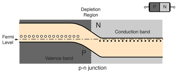
For a p-n junction at equilibrium, the fermi levels match on the two sides of the junctions. Electrons and holes reach an equilibrium at the junction and form a depletion region. The upward direction in the diagram represents increasing electron energy. That implies that you would have to supply energy to get an electron to go up on the diagram, and supply energy to get a hole to go down.

对于平衡的p-n结,费米能级在结的两侧相匹配。电子和空穴在结处达到平衡,并形成耗尽区。图中向上方向表示电子能量的增加。这意味着要将电子向上移动到图中,需要供给能量;要将空穴向下移动,也需要供给能量。
Index

Semiconductor concepts

Semiconductors for electronics
索引 半导体概念 半导体在电子学中的应用
 
HyperPhysics***** Condensed Matter
HyperPhysics ***** 凝聚态物理
R Nave
Go Back
返回


P-N Energy Bands

P-N 能带

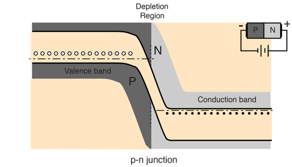
To reverse-bias the p-n junction, the p side is made more negative, making it "uphill" for electrons moving across the junction. The conduction direction for electrons in the diagram is right to left, and the upward direction represents increasing electron energy.

为反向偏置p-n结,p区被使其更负,使电子跨越结的方向变为‘ uphill’。图中电子的导电方向是右到左,向上方向表示电子能量的增加。
Index

Semiconductor concepts

Semiconductors for electronics
索引 半导体概念 半导体在电子学中的应用
 
HyperPhysics***** Condensed Matter
HyperPhysics ***** 凝聚态物理
R Nave
Go Back
返回


P-N Energy Bands

P-N 能带

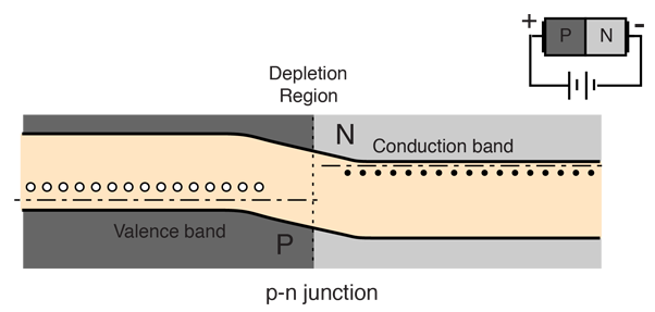
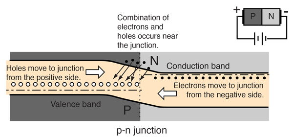
To forward bias the p-n junction, the p side is made more positive, so that it is "downhill" for electron motion across the junction. An electron can move across the junction and fill a vacancy or "hole" near the junction. It can then move from vacancy to vacancy leftward toward the positive terminal, which could be described as the hole moving right. The conduction direction for electrons in the diagram is right to left, and the upward direction represents increasing electron energy.

为使p-n结正向偏置,p区需被设为更正,这样电子在结处的运动就是‘ downhill’。一个电子可以穿过结并填满接近结处的空位或‘空穴’。它然后可以向正极方向移动,从一个空位到另一个空位,这可以描述为空穴向右移动。图中电子的导电方向是右到左,向上方向表示电子能量的增加。
Show more detail on conduction under forward bias.
在正向偏置下导电的更多细节
Index

Semiconductor concepts

Semiconductors for electronics
索引 半导体概念 半导体在电子学中的应用
 
HyperPhysics***** Condensed Matter
HyperPhysics ***** 凝聚态物理
R Nave
Go Back
返回


Forward Biased Conduction

正向偏置导电

When the p-n junction is forward biased, the electrons in the n-type material which have been elevated to the conduction band and which have diffused across the junction find themselves at a higher energy than the holes in the p-type material. They readily combine with those holes, making possible a continuous forward current through the junction.

当p-n结正向偏置时,n型材料中被提升到导带的电子扩散过结界后,其能量高于p型材料中的空穴。它们很容易与这些空穴结合,从而使得结界中持续有正向电流通过。
Show more detail about charge carriers.
关于载流子的更多细节。
Index

Semiconductor concepts

Semiconductors for electronics
索引 半导体概念 半导体在电子学中的应用
 
HyperPhysics***** Condensed Matter
HyperPhysics ***** 凝聚态物理
R Nave
Go Back
返回


Forward Biased Conduction

正向偏置导电

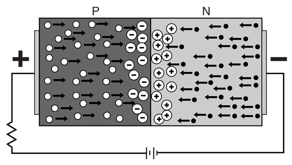
The forward current in a p-n junction when it is forward-biased (illustrated below) involves electrons from the n-type material moving leftward across the junction and combining with holes in the p-type material. Electrons can then proceed further leftward by jumping from hole to hole, so the holes can be said to be moving to the right in this process.

在p-n结正向偏置时(如图所示), forward电流涉及从n型材料中的电子向左移动穿过结并与p型材料中的空穴结合。电子随后可以跳到下一个空穴,因此可以说空穴向右移动。
Index

Semiconductor concepts

Semiconductors for electronics
索引 半导体概念 半导体在电子学中的应用
 
HyperPhysics***** Condensed Matter
HyperPhysics ***** 凝聚态物理
R Nave
Go Back
返回