Intrinsic Semiconductor本征半导体
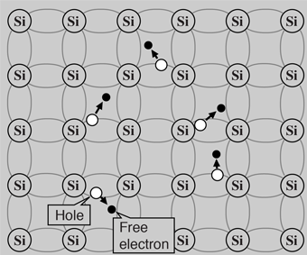
A silicon crystal is different from an insulator because at any temperature above absolute zero temperature, there is a finite probability that an electron in the lattice will be knocked loose from its position, leaving behind an electron deficiency called a "hole". 一个硅晶体与绝缘体不同,因为在任何高于绝对零度的温度下,都有一定的概率使晶格中的一个电子脱离原位置,留下一个称为‘空穴’的电子空缺。
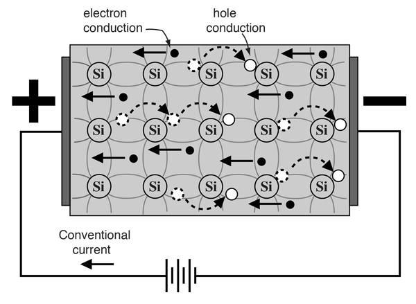
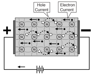
If a voltage is applied, then both the electron and the hole can contribute to a small current flow. 若施加电压,则电子和空穴均可贡献于微小的电流流动。
|
Index Semiconductor concepts 索引 半导体概念 | |||
|
Go Back
返回 |
Semiconductor Current半导体电流
![]()
在本征半导体中,电子和空穴都对电流流动有贡献。 |
Index Semiconductor concepts 索引 半导体概念 | ||
|
Go Back
返回 |
Semiconductor Current半导体电流
The current which will flow in an intrinsic semiconductor consists of both electron and hole current. That is, the electrons which have been freed from their lattice positions into the conduction band can move through the material.
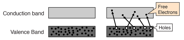
The current flow in an intrinsic semiconductor is influenced by the density of energy states which in turn influences the electron density in the conduction band. This current is highly temperature dependent. 在本征半导体中,电流的流动受能量态密度的影响,而这种能量态密度又影响导带中的电子密度。这种电流高度依赖于温度。
在本征半导体中流动的电流由电子电流和空穴电流共同组成。也就是说,那些从晶格位置中释放出来进入导带的电子可以在材料中移动。 |
Index Semiconductor concepts 索引 半导体概念 | ||
|
Go Back
返回 |
Electrons and Holes电子与空穴
In an intrinsic semiconductor like silicon at temperatures above absolute zero, there will be some electrons which are excited across the band gap into the conduction band and which can produce current. When the electron in pure silicon crosses the gap, it leaves behind an electron vacancy or "hole" in the regular silicon lattice. Under the influence of an external voltage, both the electron and the hole can move across the material. In an n-type semiconductor, the dopant contributes extra electrons, dramatically increasing the conductivity. In a p-type semiconductor, the dopant produces extra vacancies or holes, which likewise increase the conductivity. It is however the behavior of the p-n junction which is the key to the enormous variety of solid-state electronic devices. 在温度高于绝对零度时,像硅这样的本征半导体中,有些电子会被激发跨越带隙进入导带,并能够产生电流。当纯硅中的电子跨越带隙时,它会在常规的硅晶格中留下一个电子空位或‘空穴’。在外部电压的影响下,电子和空穴都可以在材料中移动。在n型半导体中,掺杂剂贡献额外的电子,显著提高了导电性。在p型半导体中,掺杂剂产生额外的空位或空穴,同样提高了导电性。然而,p-n结的行为才是固态电子器件种类繁多的关键。
![]()
|
Index Semiconductor concepts 索引 半导体概念 | ||
|
Go Back
返回 |