Tunnel Diode Characteristic
隧道二极管特性
In 1957, Esaki, Kurose and Suzuki discovered that quantum mechanical tunneling of electrons could be achieved in a solid state diode. Josephson had discovered tunneling characteristics in the Josephson junction for superconductors. Esaki and Josephson shared the 1973 Nobel Prize for these discoveries.
| In the case of the tunnel diode, the conditions for tunneling were achieved by more heavily doping the semiconductors associated with the pn junction. With germanium or gallium arsenide the depletion layer at the junction was very narrow, and permitted electrons to tunnel across the barrier. For very low reverse voltages through small positive voltages, the tunneling increased and the junction acted like a conductor.
在隧道二极管的情况下,通过更 heavily doping 与 pn 结相关的半导体,实现了隧道效应。使用锗或砷化镓时,结处的耗尽层非常狭窄,允许电子穿过势垒。对于非常低的反向电压或小的正向电压,隧道效应增强,结 behaves like a conductor。 |
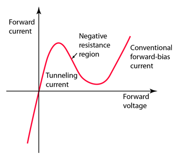 |
1957年,Esaki、Kurose和Suzuki发现电子在固体二极管中的量子力学隧穿效应。Josephson在超导体的结中发现了隧穿特性。Esaki和Josephson因这些发现共享了1973年诺贝尔奖。 For small forward bias, electrons tunnel across the depletion region from the P to the N side and fill states in the conduction band on the N-side. They align with hole states on the P-side. With increasing forward voltage, there is increasing misalignment and the current begins to drop with increasing forward voltage, producing a "negative resistance" behavior. For higher forward voltages, the junction begins to act like a normally forward biased diode, but the negative resistance regime was found to be very useful in producing oscillators.
在小正向偏置下,电子从P区隧道穿过耗尽区到N区,并在N区的导带中填充状态。它们与P区的空穴状态对齐。随着正向电压的增加,这种对齐程度逐渐减小,电流开始随着正向电压的增加而下降,产生一种‘负电阻’行为。对于更高的正向电压,结开始像通常正向偏置的二极管一样工作,但负电阻区域被发现非常有用,可用于产生振荡器。 Tunnel diode oscillators were found to be very useful through the 1970s as high-frequency oscillators and found use in the space program. They have since been mostly replaced with a variety of other oscillator types.
通过1970年代,隧道二极管振荡器作为高频振荡器被发现非常有用,并在太空计划中得到应用。它们此后大多被各种其他类型的振荡器所取代。 |
Index
Semiconductor concepts
Semiconductors for electronics
Electronics concepts
Tunnel diode, Wiki
Floyd, Electronic Devices,
Ch 3-5
索引 半导体概念 半导体在电子学中的应用 电子学概念 隧道二极管,维基百科 Floyd,电子器件,第3-5章 |