Bilingual edition: English is preserved and Chinese follows each unit. Terminology uses the confirmed v20260916 glossary; automated semantic review remains traceable.
中英双语版:英文原文完整保留,中文紧随对应单元;术语采用 v20260916 确认表,自动语义审校结果可追溯。

Transistor AND Gate

晶体管与门
AND Gate
与门
OR Gate
或门
NAND Gate
与非门
NOR Gate
Double Transistor
NOR逻辑门双晶体管
NOR Gate
Single Transistor
NOR 逻辑门 单晶体管

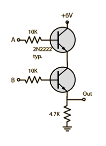
The use of transistors for the construction of logic gates depends upon their utility as fast switches. When the base-emitter diode is turned on enough to be driven into saturation, the collector voltage with respect to the emitter may be near zero and can be used to construct gates for the TTL logic family. For the AND logic, the transistors are in series and both transistors must be in the conducting state to drive the output high.

晶体管用于构建逻辑门取决于它们作为快速开关的实用性。当基极-发射极二极管被足够导通以进入饱和区时,集电极电压相对于发射极可能接近零,可以用于构建TTL逻辑家族的逻辑门。对于与逻辑,晶体管是串联的,两个晶体管都必须处于导通状态才能将输出拉高。
Basic Gates
基本逻辑门
Index

Electronics concepts

Digital Electronics

Reference
Mims
Digital Logic Circuits
索引 电子概念 数字电子 参考 数字逻辑电路
 
HyperPhysics*****Electricity and magnetism
HyperPhysics ***** 电磁学
R Nave
Go Back
返回


Transistor OR Gate

晶体管或门
AND Gate
与门
OR Gate
或门
NAND Gate
与非门
NOR Gate
Double Transistor
NOR逻辑门双晶体管
NOR Gate
Single Transistor
NOR 逻辑门 单晶体管

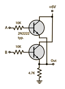
The use of transistors for the construction of logic gates depends upon their utility as fast switches. When the base-emitter diode is turned on enough to be driven into saturation, the collector voltage with respect to the emitter may be near zero and can be used to construct gates for the TTL logic family. For the OR logic, the transistors are in parallel and the output is driven high if either of the transistors is conducting.

晶体管用于构建逻辑门取决于它们作为快速开关的用途。当基极-发射极二极管被导通 enough 以进入饱和区时,集电极电压相对于发射极可能接近零,可以用来构建TTL逻辑家族的逻辑门。对于或逻辑,晶体管是并联的,如果其中任何一个晶体管导通,输出就会被驱动为高电平。
Basic Gates
基本逻辑门
Index

Electronics concepts

Digital Electronics

Reference
Mims
Digital Logic Circuits
索引 电子概念 数字电子 参考 数字逻辑电路
 
HyperPhysics*****Electricity and magnetism
HyperPhysics ***** 电磁学
R Nave
Go Back
返回


Transistor NAND Gate

晶体管NAND门
AND Gate
与门
OR Gate
或门
NAND Gate
与非门
NOR Gate
Double Transistor
NOR逻辑门双晶体管
NOR Gate
Single Transistor
NOR 逻辑门 单晶体管

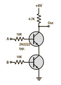
The use of transistors for the construction of logic gates depends upon their utility as fast switches. When the base-emitter diode is turned on enough to be driven into saturation, the collector voltage with respect to the emitter may be near zero and can be used to construct gates for the TTL logic family. For the NAND logic, the transistors are in series, but the output is above them. The output is high unless both A and B inputs are high, in which case the output is taken down close to ground potential.

晶体管用于构建逻辑门的用途取决于它们作为快速开关的实用性。当基极-发射极二极管被足够导通以进入饱和区时,集电极电压相对于发射极可能接近零,可以用于构建TTL逻辑家族的门。对于NAND逻辑,晶体管是串联的,但输出在它们之上。除非A和B输入都为高,否则输出保持高电平,而在这种情况下,输出会被拉低到接近地电势。
Basic Gates
基本逻辑门
Index

Electronics concepts

Digital Electronics

Reference
Mims
Digital Logic Circuits
索引 电子概念 数字电子 参考 数字逻辑电路
 
HyperPhysics*****Electricity and magnetism
HyperPhysics ***** 电磁学
R Nave
Go Back
返回


Transistor NOR Gate

晶体管NOR门
AND Gate
与门
OR Gate
或门
NAND Gate
与非门
NOR Gate
Double Transistor
NOR逻辑门双晶体管
NOR Gate
Single Transistor
NOR 逻辑门 单晶体管

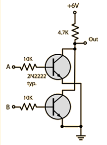
The use of transistors for the construction of logic gates depends upon their utility as fast switches. When the base-emitter diode is turned on enough to be driven into saturation, the collector voltage with respect to the emitter may be near zero and can be used to construct gates for the TTL logic family. For the NOR logic, the transistors are in parallel with the output above them so that if either or both of the inputs are high, the output is driven low.

晶体管用于构建逻辑门取决于它们作为快速开关的实用性。当基极-发射极二极管被足够导通以进入饱和区时,集电极电压相对于发射极可能接近零,可以用来构建TTL逻辑家族的逻辑门。对于NOR逻辑,逻辑门的输出位于两个晶体管的上方并联,因此如果任一或两个输入为高电平,输出将被驱动为低电平。
Basic Gates
基本逻辑门
Index

Electronics concepts

Digital Electronics

Reference
Mims
Digital Logic Circuits
索引 电子概念 数字电子 参考 数字逻辑电路
 
HyperPhysics*****Electricity and magnetism
HyperPhysics ***** 电磁学
R Nave
Go Back
返回


Transistor NOR Gate

晶体管NOR门
AND Gate
与门
OR Gate
或门
NAND Gate
与非门
NOR Gate
Double Transistor
NOR逻辑门双晶体管
NOR Gate
Single Transistor
NOR 逻辑门 单晶体管

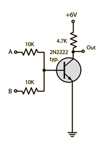
The use of transistors for the construction of logic gates depends upon their utility as fast switches. When the base-emitter diode is turned on enough to be driven into saturation, the collector voltage with respect to the emitter may be near zero and can be used to construct gates for the TTL logic family. In this alternative way to achieve NOR logic, only one transistor is used with the two inputs tied to its base through resistors. If either or both of the inputs is high, the output is driven low.

晶体管用于构建逻辑门取决于其作为快速开关的用途。当基极-发射极二极管被足够导通以进入饱和区时,集电极电压相对于发射极可能接近零,可以用于构建TTL逻辑家族的逻辑门。在这一替代方法中,仅使用一个晶体管,两个输入通过电阻连接到其基极。如果任一或两个输入为高电平,输出将被驱动为低电平。
Basic Gates
基本逻辑门
Index

Electronics concepts

Digital Electronics

Reference
Mims
Digital Logic Circuits
索引 电子概念 数字电子 参考 数字逻辑电路
 
HyperPhysics*****Electricity and magnetism
HyperPhysics ***** 电磁学
R Nave
Go Back
返回